
What Role Do Drill Holes Play in PCB Board Fabrication?
Drill Holes Play in PCB Board Fabrication
A key role that drill holes play in PCB board fabrication is to help create connections between different layers. This requires precise hole placement, size and cleanliness. To achieve these requirements, the drill process uses a computer-controlled machine that is programmed with a data set from a Gerber file. The drill machine then executes the commands based on the specified XY coordinates for each hole. Drilling can be done using a variety of techniques, depending on the design and hole sizes. A common technique is controlled depth drilling (CDD). The CDD process limits the drill bit penetration, which can be useful for creating blind vias or buried vias on multilayer boards.
The drilled PCBs are then cleaned to remove any debris or burrs from the drill site. They are also inspected for quality. This inspection can include a visual assessment, an electrical test or a cross-section analysis. The final step is the copper plating of the holes. This is done in a copper bath that has high throwing power, which enables the solution to reach into tiny and deep holes and deposit copper inside of them. This ensures consistent copper coverage in the holes and prevents short circuits.
A common mistake during the drilling process is the over-drilling of the holes. The over-drilling can damage the pcb board fabrication and cause a number of other problems, including uneven copper plating and insufficient conductivity. Another issue is the emergence of burrs around the edges of the holes. These burrs can contaminate the copper layer and affect the integrity of the circuit board.
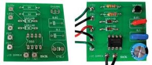
What Role Do Drill Holes Play in PCB Board Fabrication?
Drilling can produce a smear, which is caused by the high-temperature decomposition of bonding agents in the laminate system. The smear needs to be removed to ensure that the copper plate extends into the hole and contacts the underlying layers. The smear can be removed by chemical de-smear or plasma etching. For high-reliability circuit boards, a process called etch back is done with potassium permanganate etchant or nitric acid plasma. This etchback removes the resin and glass fibers from around the hole and allows for a more reliable connection between the copper layers and the underlying components or fasteners.
In addition to the above steps, a thorough cleaning is needed after the etching and plating process. This is to prevent any residuals from interfering with the subsequent manufacturing steps. Once the PCB is cleaned, it is ready for assembly.
In order to assemble the PCB, it must first be aligned. To do this, the X-ray machine locates the proper drill targets and registration holes are drilled to secure the stack before the series of more specific holes is drilled. The registration holes also help to align the inner and outer layers of the PCB for the insertion of leaded aspects. Once the PCB is assembled, it can be tested to verify its functionality and performance. A key test is the electrical testing, which can reveal issues such as poor connectivity or impedance.



Leave a Comment